


Products
HDI PCB
- Layers
- 4-20 layers
- Min. Trace Width/Space
- 2mil/2mil
- Laser Via Diameter
- 0.075mm
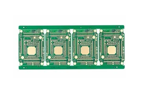
Relevant production base
SUNKING JI AN CIRCUITS ELECTRONICS CO., LTD.
Technical Specifications
| Specification | Value |
|---|---|
| Layers | 4-20 layers |
| Min. Trace Width/Space | 2mil/2mil |
| Laser Via Diameter | 0.075mm |
| Layer-to-Layer Registration | ±25μm |
| Build-Up Structure | 1+N+1 to 5+N+5 |
| Base Material | FR-4/BT/ABF |
Product Features
- Laser microvias
- Fine-line circuitry
- High-density routing
- Thin boards
Applications
Smartphones
Tablets
Wearable Devices
Digital Cameras
Laptops
Automotive Electronics
FAQ
What is the minimum via size?
- Minimum laser-via diameter 0.075 mm.
How many HDI build-ups are supported?
- We support 1+N+1 to 5+N+5 any-layer interconnection structures, with 5+N+5 HDI available in volume production.
What is the minimum trace/space?
- Minimum trace/space 2 mil / 2 mil.
Related Products
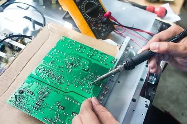
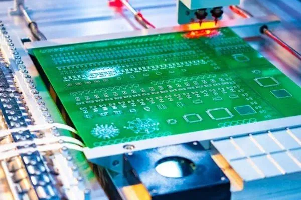


HDI step window
| Stage | Steps | Note |
|---|---|---|
| Sample / development | 1–5 steps | ≥6 steps require dedicated review |
| Volume production | 1–3 steps | Higher steps confirmed via DFM |
- Any-layer and similar complex interconnect enter engineering review against stack-up and reliability needs.
HDI process control focus
- Coordinate laser microvias (min. 0.075 mm) with mechanical holes (min. finished 0.15 mm)
- Confirm blind/buried via stack-up, build-up sequence and lamination registration window
- Match via fill / resin plug plan with surface finish (in-house ENIG / OSP / resin-plug lines)
- Design to the public 2/2 mil minimum window; actual limits tighten with copper weight and construction
HDI inspection focus
- Inner & outer layer 100% AOI
- Flying probe for prototypes; fixture test for volume
- ENIG nickel/gold thickness via XRF
- Impedance boards verified with TDR coupons
- Multilayer X-ray registration; microsection sampling for stack-up
- Delivery yield 99.8%; scrap controlled below 0.3%
- Microvia/blind-via microsection sampling for wall and dielectric integrity
- Resin-plug / fill flatness check before solder mask and finish
Typical application context
Telecom & modules
- Telecom module boards and optical-module-related HDI.
Automotive electronics
- Automotive-related PCB manufacturing under IATF 16949 (certified scope excludes product design).
Compact industrial & devices
- Space-constrained designs needing blind/buried vias to shrink layer count or size.
Project inputs & review
- Gerber/ODB++ and fabrication drawing
- Blind/buried/microvia structure notes and stack-up
- Material P/N, impedance requirements and acceptance criteria
- Quantity, schedule and sample vs volume stage
Need a quote for HDI PCB?
Upload your Gerber files and we'll quote within 1 hour for simple boards, 24 hours for complex builds.
Get Quote Now