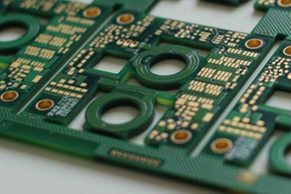
Heavy copper does not leave a plane, it leaves a terrain
On a standard board the copper layer reads visually as a thin film sitting on the substrate. There is of course a height difference between trace and substrate, but relative to the mask layer going on next, that difference is secondary.
Heavy copper is different. Per the three-tier specification table on the capabilities page, maximum outer and inner copper runs 3oz (standard), 12oz (advanced), >12oz (R&D); our claim register confirms the >12oz figure as the standing statement, with 16oz and 18oz already built in volume. Every step up in copper weight raises the copper further above the substrate. At this scale, copper stops being "a pattern on a surface" and becomes a raised feature with a defined sidewall.
This article gives no micron figure for that step height. It varies with copper weight, etch process and whether the gaps are resin filled, and it has to be confirmed in engineering review. The qualitative conclusion is enough for everything that follows:
A raised feature with a sidewall means every layer going on afterwards has to cover three distinct geometries at once: the top of the feature, the sidewall of the feature, and the substrate floor between features. The three positions do not present the same conditions, so they will not receive the same coverage.
Which capabilities each step up in copper weight compresses — layer count, board thickness, impedance — is already covered in 3oz vs 6oz vs >12oz copper weight tiers and is not repeated here. This article follows one thread only: what that step does to solder mask and surface finish.
Mask thickness is necessarily unequal across three positions
Solder mask ink flows when it is printed. A flowing material meeting a raised feature does two things: it runs toward the low ground, and it thins at the sharp corners of the feature.
The result is three states on the same board:
The floor between features. Ink collects here, so this is where mask is thickest. Thick is not itself a defect, but noticeably heavy mask on the floor pulls on overall board thickness and flatness, which has to be reconciled against the tolerance page.
The top of the feature. The top generally takes acceptable coverage, but it is also the position most exposed to handling and to downstream processes.
The sidewall, especially the upper corner. This is the thinnest position and the real risk point for heavy copper mask. If sidewall mask thins past the point of continuous insulating coverage, the copper is exposed. What exposed copper means in assembly and in service does not need elaborating.
So the heavy copper mask question is not "is the mask thick enough" — it is "is the thinnest position thick enough". The usual engineering answer involves additional print passes, which is why heavy copper mask cannot be scheduled on standard-board cadence. How many passes and in what sequence is a process parameter, confirmed in engineering review, and not published here.
Mask dams: the first thing that stops working on heavy copper
A solder mask dam is the narrow strip of mask between two adjacent pads. Its job is to stop solder migrating from one pad to the next at reflow.
On a standard board the difficulty is width — the tighter the pitch, the thinner the strip. On heavy copper there is a second difficulty: that strip has to span a stepped terrain, with a downhill slope on each side.
Which produces the most characteristic heavy copper conflict. Past a certain copper weight, at certain pitches, the dam either cannot be formed or is formed too thin to rely on. The engineering response is a binary choice: open the pitch up and give the mask room, or abandon the dam and transfer solder control to stencil aperture design and the soldering process. That choice belongs to the design stage. The line has no third option.
This is also the second reason the heavy copper page puts minimum trace width at 6mil. That number is not only the result of etch undercut — it is simultaneously the boundary where mask can still form at that spacing. Copper thickness options and design rules discusses these limits from the copper side; this article supplies the mask side.
Large copper areas: here the problem inverts
Heavy copper boards commonly carry large copper areas — current paths, heat spreading, flooded planes. On those areas the mask problem is not thinness. It is two other things.
Wrinkling and adhesion. Across an unbroken copper area with no pattern relief, mask has little geometry to key into, while copper and mask expand differently under heat. As the board moves through bake and later thermal processes, stress in a large mask field has nowhere to relieve.
Thickness uniformity. A large copper area is relatively flat in itself, but its boundary is a step running the entire perimeter. As mask pushes in from outside the copper area, that perimeter is the sidewall problem again — just much longer.
What the design side can do is define an opening strategy for large copper areas: what must be covered, what may open, where thermal pads go. That belongs on the drawing. "Solder mask: green" is not a specification.
Surface finish: heavy copper removes half the menu
The capabilities page lists HASL, lead-free HASL, ENIG, ENEPIG, hard gold and immersion silver. The heavy copper page lists three: HASL / ENIG / OSP.
That is not an arbitrary subset. One row of the surface finish comparison table on the capabilities page explains it:
> Pad flatness: HASL = Dome, LF-HASL = Dome, ENIG = Flat, ENEPIG = Flat, hard gold = Flat, immersion silver = Flat
> Fine pitch SMT: HASL ✗, LF-HASL ✗, ENIG ✓, ENEPIG ✓
> BGA / μBGA: HASL ✗, LF-HASL ✗, ENIG ✓, ENEPIG ✓
Dome means the solder on the pad is a mound, not a plane. Hot air solder levelling works by covering the pad in molten solder and blowing the excess off; surface tension pulls what remains into a curve. The smaller and denser the pads, the larger the relative effect — which is why the capabilities page marks HASL ✗ outright for fine pitch and BGA.
Heavy copper adds a layer to this. Heavy copper pads often connect to large copper areas or heavy conductors, and copper conducts heat. Solder levelling is a thermal process, so thin-copper and thick-copper regions on the same board do not behave the same thermally: the thicker the copper and the larger the area, the faster heat is drawn away. The spread in solder surface condition across one board widens.
So HASL on a heavy copper board is conditional on there being no fine-pitch devices and no BGA. If there are, that table takes you to ENIG — and that step is not free. ENIG is electroless nickel plus immersion gold, two layers with separate jobs; what each layer governs and where black pad comes from is covered in ENIG nickel and gold thickness and black pad control, and that thickness discussion is not repeated here. The side-by-side finish comparison sits in PCB surface finish comparison and on the surface finish page.
OSP occupies an awkward position on heavy copper: thin, flat, inexpensive, but the surface finish page also states it carries "more specific storage and reflow requirements". Heavy copper boards frequently see multiple reflows or accompany high-power device soldering, so that precondition has to be checked first.
Mixed boards: what gets sacrificed first
The genuinely difficult board looks like this — heavy copper current-carrying regions (large copper areas, heavy conductors, screw holes, busbar attachment points) alongside fine-pitch control circuitry (MCU, driver ICs, small passives) on the same board.
The two sets of requirements are in direct conflict:
| Heavy copper region wants | Fine pitch region wants | |
|---|---|---|
| Copper weight | As thick as possible | Thinner is easier for trace control |
| Surface finish | HASL is adequate and cheap | Must be Flat, i.e. ENIG |
| Solder mask | Large-area coverage, wrinkle resistance | Dams must form at tight pitch |
| Trace width | 6mil floor acceptable | Wants finer |
Both cannot be satisfied, so an order has to be set. Engineering usually ranks it like this:
- Fix the surface finish first, to the stricter side. One BGA or fine-pitch package on the board takes the whole board to ENIG. Surface finish is applied to the entire board in one pass; it cannot be zoned.
- Set trace width to the heavy copper floor. 6mil is the floor for the whole board, not "6mil in the heavy copper region only".
- Judge mask dams case by case. Which pitches can still form a dam and which cannot goes to engineering review, position by position.
- If the first three do not resolve it, change the construction. Separate heavy copper and fine pitch onto different layers, or split the board. How thick and thin copper layers are ordered and paired in the stackup is covered in heavy copper multilayer mixed-weight stackup.
Five things the design has to give up first
All five are things the design side can do and the line cannot:
- Give mask openings margin. Mask boundaries land less precisely on heavy copper than on standard boards; margin in the opening size is cheaper than rework.
- Open up tight pitches deliberately. Rather than gambling on whether a dam forms, open the spacing at those few positions during layout.
- State which dams are mandatory. Marking "dam required here" and "dam optional here" on the drawing gives review something to judge against.
- Specify an opening strategy for large copper areas. What is covered, what is opened, how thermal pads are handled. Colour is not a specification.
- Specify the finish with its conditions. "ENIG" alone is insufficient; state which pads it serves (BGA, fine pitch, connector contact surfaces) so incoming inspection has an acceptance basis.
The release side: what the two published gates each answer
Two quality control statements on the capabilities page bear directly on this article:
IPC-A-600 Class 2/3 acceptance. IPC-A-600 is the acceptability standard for printed boards, and solder mask coverage condition falls inside its scope. This article does not restate clauses. What matters is that Class 2 and Class 3 apply different thresholds to the same observation, so the acceptance class for a heavy copper board has to be stated on the drawing rather than left for incoming inspection to infer.
100% full-coverage electrical test. That gate tests continuity and isolation, not mask thickness. It catches shorts caused by exposed copper or missing mask, but it cannot catch "mask is thin but has not shorted yet". Mask coverage quality therefore lives on the visual acceptance gate; electrical test is a backstop, not a substitute.
The fuller inspection arrangement is on the quality assurance page. The material side — where FR-4 TG170/TG180 sits on heavy copper — is in the materials library.
FAQ
How many mask print passes does a heavy copper board need?
That is a process parameter that varies with copper weight, pattern density and mask type, and it is governed by the process sheet issued after engineering review. No general figure is published on this site. What is certain: heavy copper mask cannot be scheduled on standard-board cadence, because what has to be guaranteed is coverage at the thinnest position (the upper corner of the sidewall), not average thickness.
Can a heavy copper board use HASL?
Yes, provided there are no fine-pitch devices and no BGA. The surface finish table on the capabilities page marks HASL and LF-HASL ✗ in both the fine pitch SMT and BGA/μBGA columns, because their pad flatness is Dome rather than Flat. Heavy copper adds one more factor: copper weight and large copper areas widen the thermal spread during solder levelling. If fine pitch is present, that table takes you to ENIG.
Why is minimum trace width 6mil on heavy copper when the capabilities page says 2mil?
6mil is the heavy-copper-specific floor on the heavy copper page; 2mil/2mil is the site-wide R&D-tier window on the capabilities page. They do not conflict — the latter does not apply to heavy copper construction. The retreat is driven by two things at once: side etch grows with copper thickness (see heavy copper etch compensation), and mask cannot form reliably at tighter spacing.
If the mask dam cannot be formed, can the stencil compensate?
Partly. Once the dam is abandoned, responsibility for controlling solder migration moves to stencil aperture design and the soldering process. That is a workable approach, but it is process compensation, not an equivalent substitute — a dam is a physical barrier, while the stencil controls solder volume. Whether it is acceptable has to be reviewed per package and per pitch.
Is mask wrinkling on large copper areas a yield issue?
It behaves more like a design input issue. An unbroken copper field gives mask little geometry to key into, and copper and mask expand differently, so stress has nowhere to relieve. Defining an opening strategy at design stage is more effective than adjusting process afterwards.
Beyond "ENIG", what else does the drawing need?
At minimum: which pad types the finish serves (BGA, fine pitch, connector contact surfaces), the acceptance class (IPC-A-600 Class 2 or Class 3), and whether heavy copper and fine pitch regions carry different mask requirements. A process name on its own gives incoming inspection no acceptance basis.