


Step one: translate "layer count" into "thickness plus stackup"
Before feasibility can be discussed, the unit has to change. Layer count is design language; the shop floor only recognises thickness and stackup structure.
Finished thickness accumulates from four contributors: cores, prepreg, copper on every layer, and surface finish plus solder mask. More layers means more cores and more prepreg, so thickness almost necessarily grows with count. Holding thickness flat while adding layers means moving to thinner dielectrics — and thinner dielectric immediately touches two other things: interlayer insulation margin and impedance.
That is why "what is your maximum layer count" cannot be answered on its own. The same count is a completely different job depending on the thickness target:
- high count with a permissive thickness budget → the bottleneck lands in drilling and lamination.
- high count with thickness capped → the bottleneck lands in dielectric thickness, insulation margin and impedance control.
So every high-layer-count enquiry has to state layer count and target finished thickness as a pair. With one of them missing, the job cannot be assessed. The broader capability envelope is listed on the manufacturing capabilities page, and tolerance conventions on the tolerance page.
Constraint one: drilling aspect ratio tops out before layer count does
The most frequently underestimated constraint on a high-layer-count board sits in drilling.
Aspect ratio is the ratio of board thickness to hole diameter. SKPCB's registered standard limit for PTH aspect ratio is 10:1. What that means in practice: the thicker the board, the larger the smallest hole that can be reliably metallised. Note the order of causation — the constraint acts on hole diameter, and layer count only participates indirectly, through thickness.
This produces a chain reaction that design often misses:
- layer count rises → thickness rises;
- thickness rises → with the aspect-ratio ceiling unchanged, the smallest achievable mechanical hole gets larger;
- minimum hole gets larger → fanout and via arrays that used to fit no longer fit.
Put differently, the routing density ceiling of a high-layer-count board is not set by the layer count; it is set by thickness acting through aspect ratio. If the design insists on small holes, thickness has to be held down. If thickness cannot be held down, either larger holes or a different interconnect structure has to be accepted.
SKPCB's registered minimum mechanical hole is 0.2 mm standard (0.15 mm advanced, engineering review required); minimum laser hole is 0.1 mm standard. Laser vias follow a different path: they penetrate a single dielectric layer or a few, so they are not governed by whole-board aspect ratio. On thick high-layer-count boards the normal division of labour is therefore laser microvias carrying the high-density interconnect, mechanical holes carrying the through connections. Registered HDI depth is up to 5 stages (5+N+5) and any-layer interconnect up to 12 layers (advanced) — capabilities that exist precisely to work around whole-board aspect ratio. See HDI PCB for the board type.
The failure signature of this constraint is easy to read: discontinuous barrel plating, excessive copper-thickness difference between hole entry and hole centre, insufficient plating deep in the barrel. None of these is "the drill went wrong" — the aspect ratio was simply pushed past its window.
Constraint two: cumulative registration eats the margin
The second constraint does not live inside any single process step. It lives in how errors accumulate.
Every inner-layer core changes dimension after imaging and etching, then changes again as resin flows during lamination. Per layer the movement is small, but on a high-layer-count board the problem is that these movements do not cancel each other — they stack across layers. What eventually shows up is not "one layer drifted" but a relative offset between the outermost layers large enough that drilling cannot satisfy every layer at once.
Registration margin appears in the design as annular ring — how much copper is left between hole edge and pad edge once the drill lands on the pad. The higher the layer count, the tighter the margin allocated per layer, because the total margin is fixed while the number of contributors has grown.
SKPCB's registered hole position accuracy is ±0.05 mm (normal grade). That is the drilling capability, but registration failures on high-layer-count boards are usually not caused by drilling — drilling is where the error becomes visible, not where it is produced. Production happens in inner-layer imaging and lamination movement. This is why registration problems on these boards cannot be solved by "drilling more accurately".
Design has only two real levers:
- Budget enough annular ring. Pads on a high-layer-count board cannot be drawn to the minimum that a low-layer-count board tolerates. Annular ring is the registration budget.
- Accept zoning. Not every area on the panel needs equal registration. Concentrating critical registration demand locally is far more realistic than tightening the whole board uniformly.
Process-side registration controls (targets, compensation, sequential lamination) are covered in multilayer lamination registration control and are not repeated here.
Constraint three: thickness squeezes the lamination window
The third constraint sits in lamination, and it is often misread as "not enough press tonnage". What actually tightens is heat and flow.
Thick boards face two unavoidable physical facts in lamination:
The core heats up late. The thicker the board, the longer heat takes to reach the centre. So outer regions and the core sit at different cure stages at the same moment — the outside has started crosslinking while the centre is still flowing. Fully curing the centre requires more time or more temperature, and both of those over-cure the outside. The lamination window is whatever space is left between these two opposing demands, and the thicker the board, the narrower that space becomes.
Resin has further to travel. Every layer needs resin to fill the gaps between features. With many layers and thin dielectric per layer, resin travels longer paths through narrower channels. Too little flow leaves interlayer fill incomplete; too much flow squeezes the dielectric thin, so thickness and impedance both drift.
Together these explain the two most typical failure modes on thick high-layer-count boards: delamination or incomplete interlayer fill (insufficient flow and cure) and dielectric thickness scatter (excess flow and uneven pressure distribution). Prevention of the first is covered in lamination void and delamination prevention; how uneven copper amplifies warpage on thick boards is covered in multilayer copper balance and warpage control.
The three constraints are coupled — this is the part that matters
Now the opening question can be answered: why "maximum layer count" cannot be answered in isolation.
Because all three constraints share one variable — board thickness — and their demands conflict:
| Constraint you want to relax | The intuitive move | Where the cost lands |
|---|---|---|
| Drilling aspect ratio | Thin the board down (thinner dielectric) | Interlayer insulation margin and impedance tighten; narrower resin flow channels narrow the lamination window further |
| Interlayer registration | Enlarge pads / annular ring | Routing density drops, which may force more layers → thickness climbs back |
| Lamination window | Add dielectric thickness, relax the cycle | Thickness climbs → aspect ratio tops out, minimum hole diameter rises |
Every "cost" in that table lands on another row's "constraint". Achievable layer count is therefore the intersection of the three, not the individual ceiling of any one of them. That is also why a high-layer-count board needs a stackup review before a price: the review is exactly the question of whether that intersection is non-empty at the given thickness, hole size and impedance requirements.
Impedance tolerance participates in the same intersection. SKPCB's registered values are ±10% standard and ±5% advanced (engineering review required). Thinner dielectric and more layers demand tighter dielectric thickness consistency to hit the tighter grade — which routes straight back to the lamination window. See impedance control PCB for the board type.
Downstream steps change too
The three constraints above decide whether the board can be built. Downstream steps decide whether it can be released. Difficulty rises in step with layer count in several places; this is a qualitative summary only:
Electrical test. Higher layer count means more nets and more buried or blind structures, so test-point accessibility drops. Flying probe and fixture each have their range; the selection logic is in flying probe vs fixture electrical test. On high-layer-count boards this is no longer only a cost question — it becomes a question of whether the net can be reached at all.
Profiling. Routing and V-cut on thick boards are limited by tooling and stress, and tolerances are expressed differently than on thin boards. See profiling, outline routing and V-cut tolerance.
Surface finish. Thick boards spend longer under thermal and chemical exposure in the finishing line, so plating uniformity gets harder to control. Trade-offs per process are in surface finish comparison.
Warpage. Thick boards are not inherently flatter. With more layers and more thickness, internal stress from asymmetric copper is harder to relieve, so warpage control has to enter at the stackup stage.
Inputs required before quoting
A layer count on its own cannot support a quote or a feasibility call. Any of the following missing blocks the review:
- Layer count plus target finished thickness (as a pair, stating whether thickness is hard or negotiable)
- Minimum hole diameter and hole-type mix (mechanical through, laser microvia, buried/blind — minimum size and rough quantity for each)
- Impedance requirements and tolerance grade (which nets are controlled, ±10% or tighter)
- Stackup intent (which layers are signal, which are planes, any specified dielectric)
- Registration-critical areas (uniform across the panel, or locally critical)
- How outline and thickness tolerance are expressed (where on the drawing, against which datum)
- Whether the tiered capability convention is accepted (standard production values can be committed directly; higher tiers need engineering review)
With all seven supplied at once, the review can answer whether your layer count is buildable at your thickness and hole size. With layer count alone, the only possible answer is a range. Formal reviews can be submitted via the quote and engineering review entry.
What this article concludes
- Layer count is not the capability boundary; thickness is the variable all three constraints share.
- Drilling aspect ratio tops out first, acting on hole diameter and thereby on routing density.
- Registration error accumulates with layer count; drilling is the exposure point, not the source. Design's levers are annular-ring budget and zoning.
- The lamination window on thick boards is squeezed from both sides by late core heating and longer resin travel.
- The three constraints are each other's cost, so achievable layer count is their intersection — which is why stackup review precedes pricing.
FAQ
What is the maximum layer count SKPCB can build?
The registered convention is 40 layers standard production with 64 layers as the maximum. The top tier is an advanced capability requiring engineering review, not an unconditional commitment; the layer count actually achievable depends on the combination of target thickness, minimum hole size and impedance requirements.
Does a higher layer count always mean a thicker board?
With dielectric selection unchanged, yes — more layers means more cores and prepreg. Holding thickness while adding layers requires thinner dielectric, which tightens interlayer insulation margin and impedance control and narrows the lamination window. Registered finished thickness range is 0.2–6.0 mm.
Why does board thickness limit minimum hole diameter?
Because aspect ratio — thickness divided by hole diameter — has a ceiling; the registered PTH standard value is 10:1. As thickness rises, hole diameter has to rise with it to stay inside that ceiling. This is a primary source of routing-density limits on high-layer-count boards.
Can registration problems be solved by more accurate drilling?
No. Hole position accuracy is registered at ±0.05 mm (normal grade), but registration error on high-layer-count boards is produced mainly in inner-layer imaging and lamination movement. Drilling is only where it becomes visible. The effective responses are sufficient annular ring, zoning of critical registration demand, and process-side movement compensation.
Why does a high-layer-count board need a stackup review before a price?
Because aspect ratio, registration and the lamination window share board thickness as their single variable and act as each other's cost — relaxing one raises the difficulty of another. The review determines whether the intersection of the three is non-empty at your thickness, hole size and impedance requirements.
Are high layer count and HDI the same thing?
No. Layer count describes how many layers are stacked; HDI describes the interconnect method. Thick high-layer-count boards commonly use laser microvias for dense interconnect and mechanical holes for through connections, specifically to avoid the whole-board aspect-ratio limit. Registered HDI depth is up to 5 stages (5+N+5), and any-layer interconnect up to 12 layers (advanced tier).
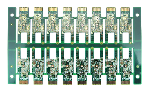
- Image alt: Top-down view of a multilayer production panel with process rails and tooling holes, showing regularly arrayed units and gold contact fingers — layer count is invisible in the finished appearance and only surfaces at drilling, registration and lamination
---