Where E-test sits in the flow: a release action, not process control
The manufacturing flow on /capabilities/ runs ten steps: 01 Cutting → 02 Inner Layer → 03 Lamination → 04 Drilling → 05 Plating → 06 Outer Layer → 07 Solder Mask → 08 Surface Finish → 09 Profiling → 10 Testing. E-test sits last, and that position defines its nature.
Process control intercepts problems between steps: after inner layer, AOI checks trace width, spacing, shorts, opens and nicks panel-by-panel against the design data; after plating, copper thickness is measured. The point of those actions is to stop a defect before it enters the next step.
E-test is not that. It runs after every process step is finished and the board is already profiled, and it answers one summary question: is the electrical connectivity of this finished board the same as the connectivity the design data calls for? It does not tell you which step went wrong. It tells you whether this board can ship.
Precisely because it sits last, defects caught at E-test are the most expensive ones — material, labour and surface finish are all already invested. Which is why none of the upstream process controls are optional: push all defect discovery to step 10 and the whole batch carries the cost.
What actually differs: where the probe position comes from
Flying probe and fixture testing both touch probes to test points and measure resistance. There is exactly one difference: whether probe position comes from the data or from a physical fixture.
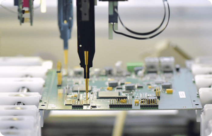
Flying probe: a handful of probes on moving arms, stepping net by net through the netlist. Test-point coordinates come straight from the design data, so it needs no physical preparation for this particular board. New board, new data, and the machine can test immediately. The ATG flying probe listed on /capabilities/ is this class of equipment.
Dedicated fixture (bed-of-nails): a jig built for one specific board, with a fixed probe at every point to be tested. The board presses down and all points make contact at once. It requires a physical fixture to be built first, but once built, each board is tested in a single press.
That yields the real differences in character:
| Flying probe | Dedicated fixture | |
|---|---|---|
| Probe position from | Design data, stepped point by point | Physical bed of nails, all contact in one press |
| Cost to change board | New data file | New fixture must be built |
| Cycle time per board | Grows with net and test-point count | Largely independent of test-point count |
| Demand on the board | Board only needs holding | Board must survive full-face press force |
Note the last row. That is the criterion most people leave out, and it has nothing to do with cost.
The three real criteria
/quality/ marks the stage for this item as "confirmed per product and order" — not boilerplate, but because more than one criterion applies and they have to be read together.
Criterion one: batch size. The intuitive one, and the main source of "flying probe for prototypes, dedicated fixtures for volume". A fixture is a one-off investment that is then reused; the larger the batch, the thinner that investment spreads, while what it saves is per-board cycle time. At a handful to a few dozen pieces, the fixture has not begun to pay back and probing directly makes more sense.
Criterion two: net and test-point count. Flying-probe cycle time grows with test-point count; fixture cycle time essentially does not. So on a board with a very large net count, even at moderate volume, cumulative probe time can already exceed the cost of building a fixture. Conversely, a sparse simple board may be comfortable on flying probe even at high volume. Batch size and test-point count have to be computed together, not one in isolation — that is where the "thousands of pieces still on flying probe" and the "small batch that needed a fixture" orders come from.
Criterion three: whether the board can take fixture pressure. The first two are arithmetic about cost and cycle time. The third is a hard constraint:
- Thin boards. The board-thickness range on
/capabilities/starts at 0.2 mm. Full-face press force on that thickness needs supporting design, not just lowering a bed of nails onto it. - Flex and rigid-flex. A flexible region has no rigid support of its own; the deflection from a fixture press cannot be carried by the board itself.
- Irregular outlines and special edge structures. Castellated holes and gold fingers need contact position and method assessed individually.
- Test points covered by solder mask, or too close together. Strictly this is not "can it be pressed" but "is there metal to touch when it is pressed" — covered in its own section below.
The conclusion from criterion three: for some boards it is not that a fixture costs more, but that the fixture route needs additional engineering assessment before it can be confirmed feasible. In those cases method selection goes back to engineering review; it cannot be auto-derived from a volume table.
What E-test can judge
Per the wording on /quality/, E-test covers two things:
Netlist continuity. Nets the design data says should be connected — are they measurably connected? This catches the open-circuit family: traces broken by over-etch, discontinuous hole-wall plating, vias that fail to connect inner layer to outer layer.
Insulation resistance. Nets the design data says should be independent — are they measurably independent? This catches the short and leakage family: etch residue, bridging from insufficient spacing, unintended interlayer conduction.
Together they form one complete judgement: the connectivity of the finished board matches / does not match the design netlist. A binary verdict, and one that covers every net on the board. That coverage is the whole value: AOI checks whether the pattern matches the design data, a microsection shows the cross-section of one hole, and E-test is the only action that verifies every net relationship on the board against the design data in one pass.
What E-test definitively cannot judge — and who owns each of those
This section matters more than method selection. Passing E-test does not mean the board is acceptable. It verifies connectivity only. Every item below is invisible to it, and each has its own owning method, all taken from the inspection-method table on /quality/:
| Invisible to E-test | Owning method | Site wording |
|---|---|---|
| Trace width, spacing, shorts, opens, nicks — pattern conformance | AOI | Panel-by-panel against the design data |
| Hole-wall condition and plating structure | Microsection | Destructive, per the confirmed sampling |
| Whether copper thickness meets requirement | Copper-thickness measurement | Five or more points per production panel, non-destructive; tightened on heavy copper |
| Whether controlled impedance is within tolerance | Test coupon + TDR | Single-ended / differential measured against stack-up design values and tolerance |
| Solder-joint interiors on assemblies (voids, bridging, collapsed balls) | X-ray | BGA and QFN on assemblies, joints hidden from view |
| Solder-mask registration and finish thickness | Imaging measurement and thickness checks | Mask registration and thickness, gold/nickel thickness on ENIG |
A few confusions worth separating out:
"E-test passed — why is impedance still wrong?" Because E-test measures continuity and insulation, connectivity at DC level; controlled impedance is a high-frequency characteristic set by the combination of trace width, dielectric thickness and dielectric constant. A trace running at 70 Ω against a 50 Ω target looks perfectly normal to E-test — it conducts, and it is insulated from everything else. Impedance has to be judged by TDR on a test coupon; the site marks impedance-controlled boards as "test coupon on impedance-controlled boards". These are two independent release conditions. See impedance test coupon verification.
"E-test passed — why do the traces look so thin?" Trace-width tolerance is ±20% (see /tolerance/); a trace on the thin side but still conducting passes E-test. Pattern conformance belongs to AOI, checked panel-by-panel against the design data. See outer-layer pattern inspection.
"E-test passed — why are there BGA opens after assembly?" Because that is not the bare board's problem domain. E-test verifies bare-board connectivity; voids and bridging inside BGA/QFN joints happen after assembly and belong to X-ray. Different inspection objects entirely.
"E-test passed — why is copper thickness tightened on heavy copper anyway?" Copper thickness sets current-carrying and thermal capability, and a trace with thin copper can still conduct perfectly. The copper range on /products/heavy-copper-pcb/ runs 3oz to >12oz; thickness on those boards is governed by five or more non-destructive measurement points per production panel, and the site states explicitly that heavy copper is tightened further.
One line to close it: E-test answers "is the connectivity right"; every other capability has its own verification action. The full method list is on PCB quality inspection methods and the quality system page; the site's standing wording is that the exact inspection set, sampling level and applicable standards are confirmed per product and order, within an IPC-A-600 Class 2 framework.
What stalls E-test or forces rework
E-test failures come in two kinds with completely different natures.
Kind one: the board really is wrong. Opens, shorts, vias that did not connect. This is what E-test is for; catching these is it doing its job.
Kind two: the board is fine but cannot be tested. Purely missing preparation, yet it stops the batch at step 10 all the same:
- Netlist does not match the Gerber. E-test judges against the design netlist. If the submitted netlist describes different connectivity than the Gerber, the result reports a batch of defects that do not exist, and the job goes back to CAM review for clarification.
- Test points covered by solder mask. The wording on
/tolerance/is: mask clearance should be 0.003" larger than the pads (mask swell), with mask registration tolerance ±0.003". When the clearance design does not leave that margin, mask can encroach on the pad edge in production and probe contact area falls short. - Test points too close together. Same page: standard mask bridge 0.004", and pads within 0.010" may need special processing. On a fixture, closely spaced test points mean adjacent probe layout needs additional assessment.
- No test point at all. Some nets have no exposed copper anywhere for a probe to touch; continuity on those nets cannot be verified.
The common trait of kind two: all of it is avoidable at design stage, and at step 10 the only option is going back upstream. Which is the practical reason for putting the E-test requirement into the order package.
Four things to submit or confirm when ordering
- A netlist, or authorisation to extract one from the Gerber. IPC-D-356 or an equivalent format is preferred. If only Gerber is supplied, authorise CAM explicitly to extract connectivity from the Gerber as the test reference and accept that extraction as the basis.
- Whether E-test is required. The wording on
/quality/is that final electrical testing and outgoing inspection are confirmed per product and order; where the order requires electrical testing, it is performed by the applicable means — flying probe for prototypes or fixtures for volume. It is an order-level confirmation, so state it when ordering. - This batch quantity and expected follow-on batches. This drives method selection directly. If the first batch is a prototype with a defined volume plan behind it, say so up front so the fixture investment can be planned once instead of decided twice.
- Any structure on the board that cannot take pressure. Boards near the 0.2 mm end of the thickness range, flex and rigid-flex constructions, castellated holes, gold fingers, irregular outlines — put these on the table at review, so the fixture route is not reassessed after the method has been chosen.
Full capability windows are on the manufacturing capabilities page and tolerance wording on the manufacturing tolerances page. With the data ready, go straight to quote and engineering review.
FAQ
Q: Is "flying probe for prototypes, dedicated fixtures for volume" a hard rule?
A: No. It is the normal practice stated on Sunking's /quality/ page, and the same page marks the stage for that item as confirmed per product and order. The actual choice weighs three criteria together: batch size, net and test-point count, and whether the board can take fixture press force. Substantial batches do sometimes stay on flying probe, and modest batches do sometimes need dedicated assessment because of structure or test-point count.
Q: Do flying probe and fixture testing give different verdicts?
A: The reference is the same — netlist continuity and insulation resistance against the same design netlist. The difference is where probe position comes from and per-board cycle time, not the nature of the verdict.
Q: If E-test passes, is the board acceptable?
A: No. E-test verifies connectivity and insulation only. Pattern conformance belongs to AOI, hole wall and plating to microsection, copper thickness to five or more non-destructive points per panel (tightened on heavy copper), controlled impedance to TDR on a test coupon, and assembly solder joints to X-ray. Outgoing release runs against the confirmed final-inspection set as a whole, of which E-test is one item.
Q: My board is 0.2 mm thin and partly flexible. Can it be E-tested?
A: E-test itself is not limited by that; the method is. A full-face fixture approach on such a board needs additional support and press assessment, so provide thickness, the extent of the flexible region and the outline at review and let engineering confirm the applicable means.
Q: I only have Gerber, no netlist. Can it be tested?
A: Yes, via CAM extracting connectivity from the Gerber, but that needs explicit authorisation at order stage and acceptance of the extraction as the test reference. If the design has specific connectivity intent on certain nets, supplying IPC-D-356 or an equivalent netlist directly avoids a reference mismatch.
Q: Can E-test find impedance out of tolerance or insufficient copper thickness?
A: No. Both can be out of tolerance while fully conducting and fully insulated. Impedance is measured by TDR on a coupon on impedance-controlled boards against stack-up design values; copper thickness is measured at five or more non-destructive points per production panel, tightened on heavy copper.