


Products
Double-Sided PCB
- Layers
- Double-sided
- Board Thickness
- 0.4mm-3.2mm
- Copper Thickness
- 0.5oz-4oz

Relevant production base
SUNKING JI AN CIRCUITS ELECTRONICS CO., LTD.
Technical Specifications
| Specification | Value |
|---|---|
| Layers | Double-sided |
| Board Thickness | 0.4mm-3.2mm |
| Copper Thickness | 0.5oz-4oz |
| Min. Trace Width/Space | 4mil/4mil |
| Min. Hole Size | 0.2mm |
| Surface Finish | HASL/ENIG/OSP/Immersion Tin |
Product Features
- Both-side routing
- Plated through-holes
- Cost-effective complexity
- Wide application range
- Standard FR-4 material
- Multiple finish options
Applications
Industrial Control
Instrumentation
Automotive Electronics
Telecom Equipment
Power Management
Security Equipment
Double-Sided PCB Gallery
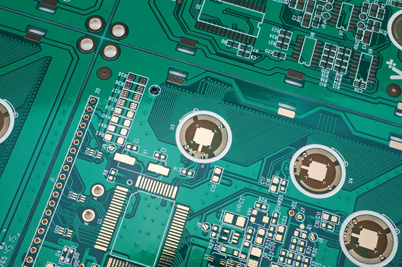
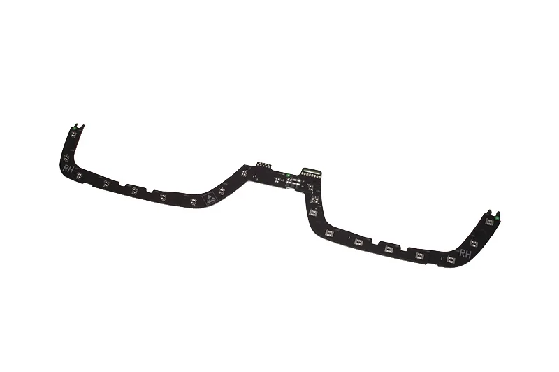
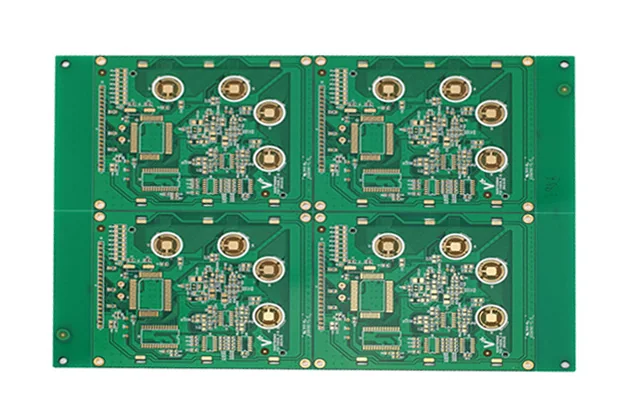
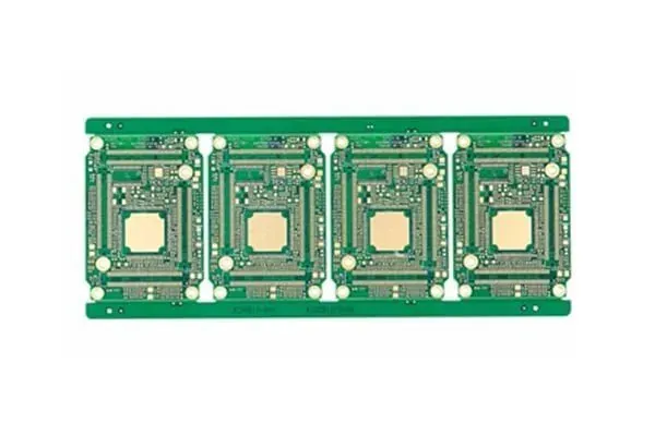
These images show component positions, contact pads and production-panel forms of double-sided PCBs. They are layout references only; copper weight, material, finish and electrical performance are confirmed from project documentation.
FAQ
How are project parameters confirmed?
- Project-specific manufacturability review against fabrication data and acceptance requirements.
Which surface finishes can be reviewed?
- Finish, supply scope and acceptance criteria confirmed in project documents.
Related Products



Need a quote for Double-Sided PCB?
Upload your Gerber files and we'll quote within 1 hour for simple boards, 24 hours for complex builds.
Get Quote Now