


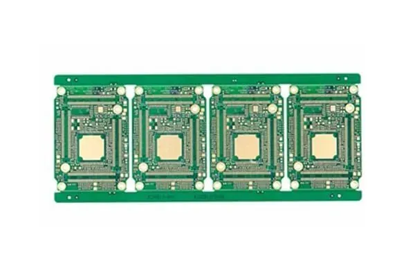
Inspection and adjudication are two different activities. Inspection answers "is something there." Adjudication answers "does it count as a defect, can it be saved, and who absorbs it." Most of our existing quality content covers the first: PCB quality inspection methods covers the techniques, the outer-layer pattern inspection checklist covers outer-layer screening, and flying probe versus fixture e-test covers test method selection. Cost and schedule, though, are driven by the second — and on most drawings it is simply blank.
This article answers only two questions on the adjudication side: what the Class level actually changes, and where the points of no rework sit.
1. Class is a contract field, not an adjective
"High-quality PCB" is not an acceptable specification because it cannot be verified. What can be verified is a standard name plus a class.
Our quality assurance page states the inspection standard as IPC-A-600 Class 2, and the capability overview lists both Class 2 and Class 3. The difference is not "more care." It is that the accept/reject boundary for the same visual feature moves. Class 2 covers products requiring continuous performance and prolonged life, and tolerates some visual deviation that does not affect function. Class 3 covers builds where interruption is unacceptable, and the same deviation may be rejected outright.
That produces one rule with direct pricing and scheduling consequences:
> If the drawing does not state a Class, acceptance defaults to Class 2. Asking for Class 3 re-adjudication afterwards swaps the entire acceptance boundary, and a completed batch may fail as a whole.
So Class has to land in writing at order confirmation, alongside two fields of equal weight: electrical test method (flying probe or fixture, confirmed per product and order) and applicable tolerances (see the manufacturing tolerance table). Without those three, inspection has nothing to adjudicate against.
2. Three possible verdicts
Once a defect is found, the outcome is one of three, and the cost spread between them is an order of magnitude.
Reworkable. Mostly coverage- and marking-layer issues where the process step itself can be redone without disturbing formed conductors or laminated structure. The cost is labour and lead time, not scrapped boards.
Not reworkable, but sortable within the array. The defect affects only some units on the production panel. Because adjudication applies to multiple identical units on one panel, failing units can be removed and the good ones shipped. Whether that route is permitted depends on whether the order accepts sorting within the array — another field that must be agreed in advance.
Scrap the batch. Wrong laminate grade, out-of-limit layer registration, and lamination delamination are structural, and no downstream step recovers them. Our quality page specifies that a data-matrix scan runs twice — at incoming material and again at lamination — precisely because wrong base material is the most expensive class of PCB error: a finished batch with the wrong dielectric constant has to be rebuilt.
3. The timeline of no rework
Laid out in order, the ten in-process checkpoints published on the quality page show which ones are one-way doors.
| Checkpoint | What it controls | After it closes |
|---|---|---|
| 01 CAM data review | Undersized openings, insufficient spacing, unbuildable stackup — flagged back to the designer | The only point where the design can still change |
| 03/04 Inner-layer imaging and AOI | AOI compares every inner-layer pattern against design data for trace width, clearance, shorts and opens | Inner-layer defects cannot be reworked after lamination. A hard fact, not a conservative position |
| 05 Multilayer lamination | Prepreg and core re-verified before pressing; finished thickness measured on every panel after pressing and logged | Registration and delamination are fixed here — see multilayer lamination registration control |
| 06 Drilling | Multilayer boards carry a dedicated coupon to check hole position relative to inner layers | Out-of-limit hole position cannot be recovered — see drilled hole quality inspection |
| 07 Copper and tin plating | Non-destructive sampling at five or more points per panel; microsection added for heavy copper and high-aspect-ratio holes | See electroplating inspection and release |
| 08 Outer-layer etching | A coupon on every panel verifies trace width against tolerance | Out-of-tolerance trace width is adjudicated on coupon measurement; the conductor is already formed |
| 09/10 Solder mask, finish, routing, final QA | Mask registration and thickness, finish thickness, outline tolerance and hole-position accuracy on a vision system | Coverage-layer issues are mostly in the reworkable class |
The way to use this table is blunt: the earlier a defect surfaces, the more options remain; the later it surfaces, the more the options collapse to sort or scrap. CAM data review is not procedural decoration — it is the only place in the line where the design itself can still move.
4. Why destructive results can only come from the coupon
Hole-wall copper uniformity, layer registration, the lamination bond line, plating structure — these require cutting the board open. Finished boards cannot be cut.
So every production panel carries its own coupon that runs the same batch through the same process. Our quality page is explicit that the coupon does three jobs: verifying trace width after outer-layer etching, checking hole position against inner layers on multilayer builds, and standing in for the finished board whenever a microsection or thermal stress test is required. Destructive testing runs on coupons, never on your delivered boards.
This corrects a common procurement assumption: a coupon report is not "data from a different board." The coupon ran in the same batch through the same process, so measuring the coupon measures the board. Impedance verification follows the same route — see impedance test coupon verification.
5. The verdict has to live in three documents
Adjudication is not an inspector's judgement call in the moment. It needs three traceable written sources:
- Drawing and order confirmation: IPC-A-600 Class level, electrical test method, whether sorting within the array is permitted, whether a coupon microsection report is required.
- Applicable tolerances: dimensional, thickness, hole-position and impedance tolerances, taken from the manufacturing tolerance table and the confirmed values for that order.
- Job quality record: each order's inspection results consolidated into its own record — laminate grade and batch, measured values at each checkpoint (copper thickness, post-lamination thickness, impedance, outline tolerance) and the tests passed. The full production record can be supplied on request.
With all three in place, a dispute has somewhere to converge. Missing one, adjudication degrades into whoever argues harder.
6. Five questions to answer before you place the order
- Acceptance to Class 2 or Class 3? Unstated means Class 2.
- Electrical test: flying probe or fixture? Prototype and volume usually differ.
- Is sorting within the array acceptable for delivery?
- Do you need a coupon microsection report, or thermal stress / solderability data?
- Do you need the full job quality record shipped with the boards?
Stating these five at the quote stage prevents discovering at final inspection that the two sides were working from different acceptance boundaries. Build options are on the product overview; base material selection is in the materials library.
FAQ
Q: What actually differs between Class 2 and Class 3?
A: Not diligence — the accept/reject boundary for the same visual feature. Class 2 covers products requiring continuous performance and prolonged life; Class 3 covers builds where interruption is unacceptable. We inspect to IPC-A-600 Class 2 by default; Class 3 must be confirmed on the order.
Q: Can an inner-layer defect be fixed?
A: Before lamination, yes. After, no. Inner-layer patterns go through AOI against design data precisely because inner-layer defects cannot be reworked once the stack is pressed.
Q: Does a coupon report represent the boards I receive?
A: Yes. The coupon ran in the same batch through the same process, so measuring the coupon measures the board. Destructive testing is done on coupons; delivered boards are not sampled.
Q: What happens if the drawing omits the Class?
A: Acceptance defaults to Class 2. Re-adjudicating to Class 3 afterwards swaps the acceptance boundary, and a completed batch may fail as a whole.
Q: Do cosmetic defects count?
A: It depends on the Class and the boundary for that specific feature. Some visual deviation that does not affect function is acceptable under Class 2 and may be rejected under Class 3 — which is exactly why the level has to be agreed first.